

In the high-stakes world of semiconductor manufacturing, the integrity of a wafer, especially a calibration or contamination wafer standard, is paramount.
Even a microscopic particle or a slight electrostatic discharge (ESD) can compromise the accuracy of metrology tools, leading to costly errors in the production line.
Protecting these sensitive components requires a rigorous approach to both storage and transport.
This article explores the technical requirements and best practices for maintaining the pristine condition of sensitive wafers.
Sensitive wafers, such as those coated with Polystyrene Latex (PSL) spheres or Silica particles, are designed with precise surface characteristics.

Their vulnerability stems from three primary threats.
Maintaining a controlled environment is the first line of defense against degradation. To ensure long-term stability, follow these storage protocols.
Wafers should always be stored within an ISO-rated cleanroom environment.

Storing them in a standard office or laboratory setting exposes them to high concentrations of particles that can bypass even the best-sealed containers over time.
Standard plastic boxes are insufficient. Use high-purity, low-outgassing containers.

Fluctuations in temperature can cause materials to expand or contract, potentially affecting the adhesion of calibration particles.

Aim for a stable temperature (typically 20-22°C) and a relative humidity of 30-50% to minimize both oxidation and static buildup.
Moving sensitive wafers between facilities or even between laboratory stations carries the highest risk of damage. Implementing a Zero-Touch philosophy is essential.
When transporting wafers outside of a cleanroom, use outer shipping containers that provide shock absorption.

Vibration-isolated transport carts should be used for internal movement to prevent the wafer from rattling inside its carrier, which can cause edge chipping.
Personnel should always wear ESD-safe gloves and use grounded wrist straps.
Ensure that all transport containers are made of static-dissipative materials to prevent the buildup of charges that could attract dust or cause a discharge event.
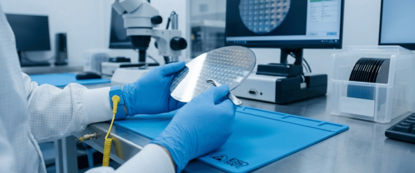
Never use manual tweezers to handle a wafer, as they apply localized pressure and can scratch the surface.

Use a specialized vacuum wand that grips the wafer from the backside or the extreme edges of the exclusion zone.
A common but overlooked threat is molecular contamination from outgassing.

Many standard packing materials release volatile organic compounds (VOCs) that can form a thin film on the wafer surface.
To ensure your metrology and calibration standards remain accurate, implement this daily checklist.
The storage and transport of sensitive wafers are not merely logistical tasks; they are critical components of contamination control and quality assurance.
By utilizing specialized carriers, maintaining environmental stability, and adhering to strict handling protocols, laboratories can ensure that their wafer standards deliver accurate, repeatable results throughout the product’s lifetime.
Investing in high-quality protection today prevents the significant costs associated with equipment recalibration and production downtime tomorrow.
Sensitive wafers should be stored in an ISO-rated cleanroom within nitrogen-purged cabinets or specialized, low-outgassing wafer shippers. This environment prevents oxidation and ensures that airborne particles do not settle on the wafer surface.
No, manual tweezers should be avoided as they apply localized pressure and can cause surface scratches. Instead, use a vacuum wand to handle the wafer from the backside or the extreme edges to maintain the integrity of the surface.
To prevent Electrostatic Discharge (ESD), always use static-dissipative transport containers and ensure that personnel wear grounded wrist straps and ESD-safe gloves. This prevents static buildup that could attract contaminants or damage the wafer.