

[et_pb_section fb_built=”1″ admin_label=”section” _builder_version=”4.16″ global_colors_info=”{}”][et_pb_row admin_label=”row” _builder_version=”4.16″ background_size=”initial” background_position=”top_left” background_repeat=”repeat” global_colors_info=”{}”][et_pb_column type=”4_4″ _builder_version=”4.16″ custom_padding=”|||” global_colors_info=”{}” custom_padding__hover=”|||”][et_pb_text admin_label=”Text” _builder_version=”4.16″ background_size=”initial” background_position=”top_left” background_repeat=”repeat” global_colors_info=”{}”]
Slowing productivity improvements and rising costs for silicon have business leaders evaluating other materials.
The path from breakthrough discovery to transformational industry applications can be a long, circuitous one. Often the first rush of possibility is followed by decades of development, refinement, and experimentation. Even then, there are no guarantees. Labs around the world are littered with once-promising technologies that never found commercial use in the market. This precedent puts executives in a difficult position when determining where and when to invest in emerging innovations. For every company that places the right bet on emerging digital technologies, there are dozens of competitors that completely miss the wave and must play catch up. Time will tell whether Kodak’s recent entrance into Bitcoin mining, for example, is an isolated move or part of a prescient long-term strategy.
Semiconductor companies find themselves in a tricky position. Regular innovation with silicon allowed the industry to generate consistent profits and consistent, impressive performance improvements for decades. More recently, companies are experiencing increased difficulty wringing more value out of silicon. This slowdown has left companies to determine what will replace silicon and when. Graphene, for example, has been heralded as a miracle material with the potential to equal or surpass silicon’s performance. However, the material’s commercialization could be up to 25 years away and will require substantial investment in both R&D and capital costs to bring it into production. With so much spending currently allocated to silicon, executives must determine the right moment to shift gears toward the next material—even when the outcome is far from guaranteed.
The challenge extends well beyond graphene; as semiconductor companies seek to identify and harness the next wave of innovation, executives must adopt a different approach. The ability to understand how seemingly disparate developments can create new business models and applications requires a more expansive perspective focused on connecting the dots and exploring new ways to apply knowledge and insights. Semiconductor executives should use this lens to shape a long-term strategy to extract value out of existing materials and technologies while monitoring nascent innovations. This mind-set will better position companies to survive both known and unknown challenges in the coming years.
Silicon, the primary material used in the semiconductor industry, has historically kept pace with Moore’s law by providing previously unimaginable progress. Disruptive and transformational technologies—advanced analytics, augmented reality, autonomous vehicles, digital, and the Internet of Things (IoT)—have been made possible by a singular element that is the namesake for the richest 50 square miles in the world. Still, serious questions are being raised about the future of silicon and its ability to continue to support innovation: three leading indicators tell the story.
Silicon offered designers and engineers a canvas that gave rise to sustained advancements in capacity and performance. A look at data from the 1970s illustrates these exponential performance improvements. However, in recent years the pace has slowed considerably. PC processing power has leveled off and increases in smartphone processor performance have begun to slow—in short, silicon is becoming mortal (Exhibit 1). These trends mean companies that built competitive advantages on continued innovation have seen their lead start to erode as other companies catch up.

Performance improvement is slowing down
Trendsetters are struggling to widen the performance improvement lead over competitors, so their ability to capture premium pricing before the rest of the market catches up is impeded. Our analysis indicates once multiple competitors enter the market, prices fall 10 to 15 percent.
Costs for semiconductor companies continue to rise as they move to next-generation fabs. To achieve performance gains, we estimate companies must increase capital spending by as much as 40 percent (given requirements for new equipment) and R&D spending by 150 percent to achieve the same throughput (Exhibit 2). The primary cause of escalating capital costs is manufacturing equipment, which has increased by about $2 billion since the industry made the transition to multipatterning. Not surprisingly, integrated device manufacturers have rapidly boosted their R&D investments for leading node technology.

Escalating capital requirements and R&D investment may inhibit further innovation
Separate from the commercial challenges, silicon’s continued growth is also uncertain because innovation has caught up to the material’s physical limitations. For example, node length is approaching the conducting channel width where performance is severely inhibited: silicon transistors will stop performing due to quantum effects of small dimensions such as tunneling, leakages, and heat issues. Limitations in lithography, instrumentation, and fabricating nanosized structures will also hinder advancements.
These three trends raise a critical question for semiconductor companies: how much should they continue to invest in silicon rather than supporting the development of innovative materials that could produce a step change in performance and sustain revenue growth?
The industry is experimenting with several exotic new materials, including silicene, germanene, and black phosphorous, but graphene is touted as having the greatest potential (Exhibit 3).
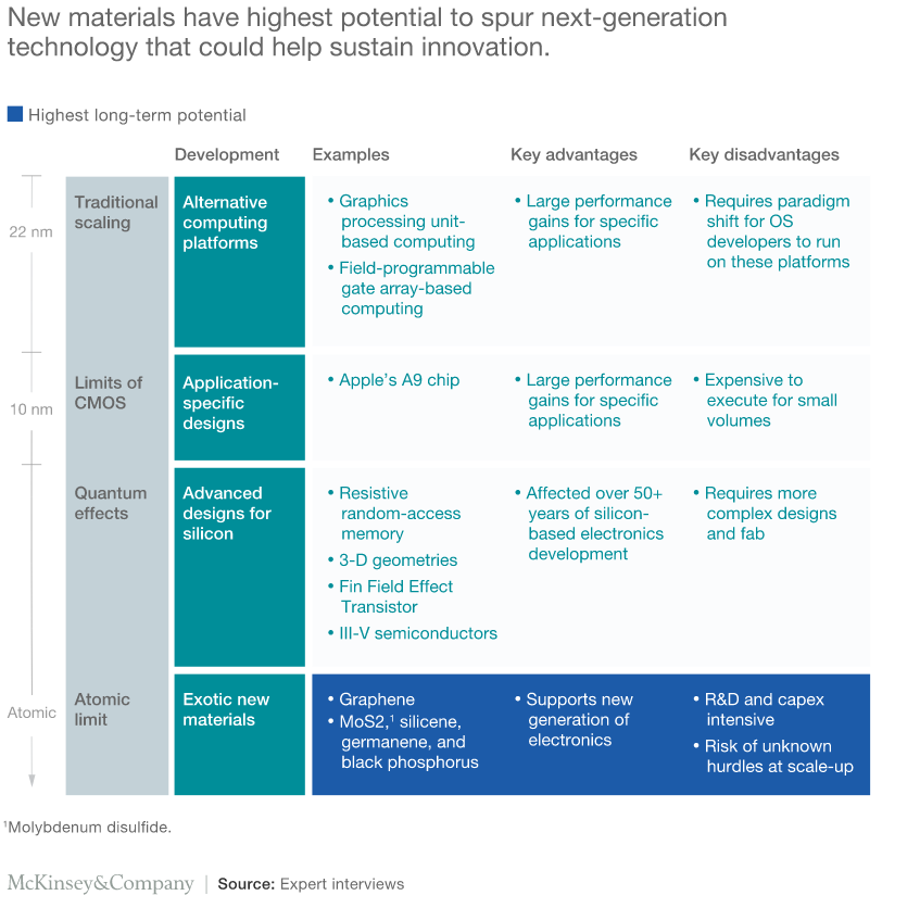
New materials have highest potential to spur next-generation technology that could help sustain innovation
The discovery of an atom-thick layer of graphene by two researchers at the University of Manchester in England in 2004, stoked expectations that it could become a superior replacement for silicon (infographic). Graphene’s properties have companies across industries salivating: its mobility is estimated to be 250 times that of silicon and its flexibility and other properties make it ideal for a range of applications, from battery technology to optoelectronics such as touch screens. Recent patents, academic papers, and research publications testify to the widespread interest in graphene.

Graphene by the numbers
Despite this promise, adoption of graphene has been elusive. So what is holding it back? We have identified four limitations, two technical and two industrial. On the technical side, band-gap engineering remains a major hurdle: without a band gap, graphene switches cannot turn off. Over the past decade, researchers have focused on addressing this issue but have yet to crack the code. In addition, graphene fabrication must generate quality crystals and be compatible with existing complementary metal-oxide semiconductor (CMOS) devices. On the industrial side, a large amount of capital is required in fabs, but semiconductor companies have most of their resources tied to current fab improvement plans. Further, an integrated value chain (including manufacturing midstream retooling) exists for silicon, but billions in investments are needed to re-create one for graphene.
Given these uncertainties, we predict graphene adoption and market growth to come in three phases—enhancer, silicon replacement, and revolutionary electronics (Exhibit 4).

We expect graphene adoption and market growth to come in three phases
In the near-term, we expect graphene to be used as an enhancer for silicon, with protective layers of graphene used to improve the reliability and performance of interconnects. Currently, 14-nanometer tantalum-nitride metal barriers are used on copper interconnects to prevent diffusion into the silicon. At gaps of less than ten nanometers, diffusion becomes a major cause of device failure—one defect per part billion results in a failure rate of around 30 percent. Graphene barriers offer several advantages over other alternatives such as ruthenium and cobalt, including better protection abilities at just one-eighth the size and with interconnect speeds around 30 percent faster.
The primary reasons for graphene’s lack of adoption are twofold. The requirements for graphene’s transfer and coating process need to be fully developed and integrated within fabrication steps. In addition, the cost of graphene must decrease significantly to enable commercial mass production. We predict it will take at least five to ten years to resolve these issues for graphene to become a viable silicon alternative.
Over the next 10 to 25 years, graphene could replace silicon as the primary material in semiconductors, assuming research discovers methods to overcome its band-gap limitations. Even then, graphene will be used in applications where its technical merits (such as high speed, low-loss requirements, small scale, and flexibility) are better suited for electronic applications than alternative materials (Exhibit 5). Our analysis calculates the total addressable market for graphene at $190 billion across data processing, wireless communications, and consumer electronics.
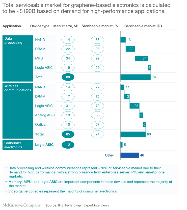
Total serviceable market for graphene-based electronics is calculated to be ~$190B based on demand for high-performance applications
Adoption is expected to follow an S-curve trend similar to other technologies, with the time frame for implementation most closely mimicking wafer adoption. Overall, optimistic scenarios show market value potential for graphene semiconductors to be around $70 billion by 2030.
History has revealed that some technologies take a long time to commercialize but can rapidly transform industries once they hit the market. In our experience, companies with a track record of casting a wide net to discover the next transformative technology tend to be more prepared to withstand industry disruptions.
Graphene’s promise is counterbalanced by the severe technical and commercial challenges discussed, which could impede its use as a silicon replacement. Therefore, when evaluating graphene’s true potential, semiconductor executives should use a structured innovation approach to evaluate their options. The innovation X-ray consists of ten questions across three categories—innovation strategy, technology disruption, and innovation practices (Exhibit 6). Addressing these questions can help business leaders get a better sense of their organization’s capabilities when pursuing innovation and support the exploration of different scenarios with or without graphene adoption. The result is a strategy that prepares organizations for dramatic, technology-driven industry change.
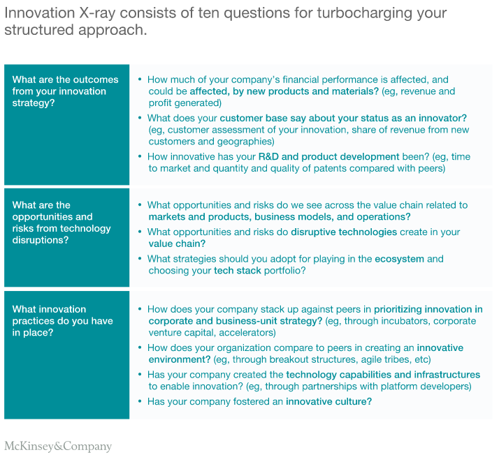
Innovation X-ray consists of ten questions for turbocharging your structured approach
After a long and productive run with silicon, executives are beginning to contemplate what might replace it and provide a similar S-curve of innovation. Graphene’s characteristics have stoked the imagination, but to date its physical limitations have kept it from being named silicon’s heir apparent. The recent history of technological innovation suggests the landscape could change rapidly—thus, executives should consider graphene as a serious contender. Regardless of the eventual outcome, semiconductor businesses can position themselves to weather technological disruption, and come out ahead, by embracing a mind-set focused on structured innovation. A world of many unknowns demands it.
Source: Graphene: The next S-curve for semiconductors? | McKinsey
[/et_pb_text][/et_pb_column][/et_pb_row][/et_pb_section]